 |
■研究開発経歴 / R&D History ・ 経歴 / History ・野鳥撮影 / Bird Photograph |
■著書 / Books ■論文 / Journals ■国際学会発表 / International Presentation ■国内学会発表 / Domestic Presentation ■解説記事 / Review articles |
|
[主要更新 ] '16-11-14: 本サイト再構築 '10-9-2: 「お知らせ」を本欄に移動 '09-2-4: 「受賞」追加 '05-6:原www.suna.cc開設 |
著 書 / Books
学術論文 / Technical Journals
国際学会発表 / International Conference Presentation
国内学会発表 / Domestic Conference Presentation
解説記事 / Review Articles
| 1. | 「半導体研究4巻:エピタキシャル成長」,西澤潤一編、熊川征治、角南英夫、寺崎健、西澤潤一共著,「光気相エピタキシャル法」,pp. 1-13(第4回半導体専門講習会予稿
集) (1969年3月25日), (株) 工業調査会、東京), 1969年。 "Semiconductor Research #4 : Epitaxial Growth," J. Nishizawa (Ed.) S. Kumagawa, H. Sunami, K. Terasaki, and J. Nishizawa(coauthor) , "Light Assisted Epitaxial Growth," pp. 1-13 Kogyochosa-kai, 1969. | 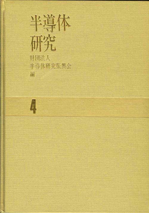 | |
| 2. | 「半導体研究4巻:エピタキシャル成長」、西澤潤一編、角南英夫、西澤潤一共著、「シリコンの気相成長層における積層欠陥の構造」:pp. 15-29、(第4回半導体専門講習会予稿集)、
(1969年3月25日,、(株) 工業調査会、東京), 1969年。 "Semiconductor Research #4 :Epitaxial Growth," J. Nishizawa (Ed.), H. Sunami and J. Nishizawa(coauthor), "Stacking Faults in Silicon Epitaxial Layer," pp. 15-29 Kogyochosa-kai, 1969. |
| |
| 3. | 「MOS LSI製造技術」、(徳山魏、橋本哲一編)、角南英夫共著、
「第1章:MOS デバイスの基本特性/第2章:トータル・プロセス」、
pp. 11-48、日経マグロヒル社、1985年。 "MOS LSI Fabrication Technologies," T. Tokuyama & N. Hashimoto(Ed.), H. Sunami(co-author), "1. MOS devices & 2. Total process,", pp. 11-48, Nikkei MacGrow Hill, 1985. | 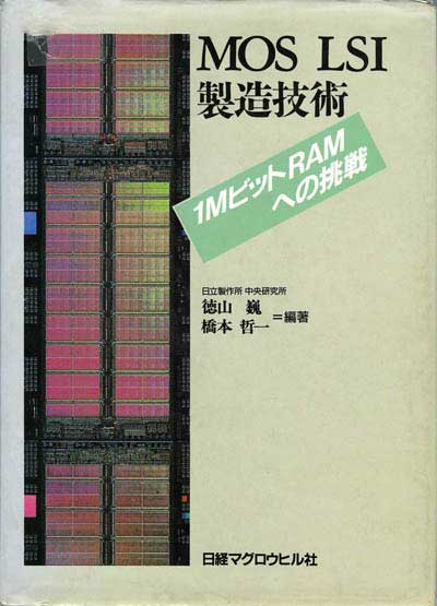 | |
| 4. | 「半導体研究24巻:超LSI技術, 10超LSI回路とプロセス」、
西澤潤一編、角南英夫、浅井彰二郎共著、「ダイナミックMOSメモリ技術」、pp.51-79、(第24回半導体専門講習会予稿集) (1986年8月15日),
(株) 工業調査会、東京), 1986年。 "Semiconductor Research #24 : VLSI Circuits and Process," J. Nishizawa (Ed.), H. Sunami & S. Asai (coauthor), "Dynamic MOS Memory Technology," pp. 51-79, Kogyochosa-kai, 1986 | 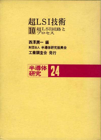 | |
| 5. | 「デバイス材料工学」,
(北田正弘,後藤和弘編), 角南英夫共著, 「第7章:集積回路材料技術」, pp. 136-155、
海文堂、1988年3月。
"Device Material Technology," M. Kitada & K. Goto (Ed.), Hideo Sunami (co-author), "7. Integrated Circuit Material Technology," pp. 136-155, Kaibundo, March 1988. | 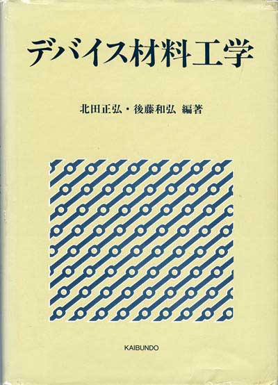 | |
| 6. | 「次世代超LSIプロセス技術(基礎編)」, (廣瀬全孝編), 角南英夫共著, 「第2節:トータル プロセス」, pp. 27-39, リアライズ社, 1988年4月. "Advanced VLSI Process Technology," Masataka Hirose(Ed.), H. Sunami (coauthor), " 2. Total process," pp. 27-39, Realize Inc., April 1988. |  | |
| 7. | 「VLSI製造技術」, (徳山薮覆、橋本哲一編)、角南英夫共著:「第1章:MOSデ バイスの基本特性, 2章:トータル・プロセス」, pp. 1-57, 日経BP社、東京、1989年1月。 "VLSI Fabrication Technologies,"T. Tokuyama & N. Hashimoto(Ed.), H. Sunami (co-author), "1. MOS devices & 2. Total process,", pp. 1-57, Nikkei BP, Jan. 1989. | 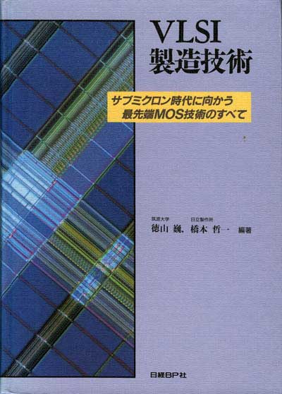 | |
| 8. | 「月刊Semiconductor World 別冊号」, 角南英夫共著,
「第1章:MOSプロセスフローチヤート - 16MDRAMを例にとって - 」,
pp. 35-41, 1989年11月2日. "Supplement to Monthly Semiconductor World,", Hideo Sunami (co-author), "1. MOS process flow chart -16M DRAM-,"pp. 35-41, Semiconductor World, Nov. 2, 1989. |  | |
| 9. | 「Encyclopedia of Applied Physics, Vol 17」,
米国物理学会, Hideo Sunami共著, "Semiconductor-Device Integration," pp. 181-198, 1996年. "Encyclopedia of Applied Physics," Vol. 17 , AIP, Hideo Sunami(co-author), "Semiconductor-Device Integration," pp. 181-198, 1996. | 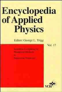 | |
| 10. | 「半導体大辞典」,(工業調査会, 菅野卓雄, 川西剛監修),
角南英夫共著:「自己整合技術」, pp. 622-625, 工業調査会,1999年12月。 "Dictionary of Semiconductor Technology, Industry,", Kogyochosa-kai, T. Sugano & G. Kawanoishi (Ed.), Hideo Sunami(co-author), "Self-align technology," pp.622-625, Kogyochosa-kai, Dec. 1999. |  | |
| 11. | 「次世代ULSIプロセス技術」, (広瀬全孝編),
角南英夫共著:「第1章:次世
代ULSIとは, 2章:ULSI集積化
技術」, pp. 3-57,
リアライズ社, 2000年2月。 "Advanced ULSI Process Technology," Masataka Hirose(Ed.), H. Sunami (coauthor), "1. Advanced ULSI, 2. Integration process, " pp. 3-57, Realize Inc., February 2000. | 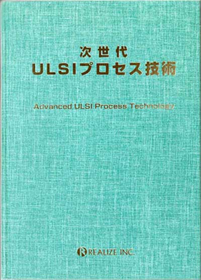 | |
| 12. | 「マイクロエレクトロニクスにおける高分子材料」, ((社)高分子学会編),
角南英夫共著, 「第1章: ULSIの将来展望と高分子材料への期待」, pp. 3-36,
(社)エヌ・ティー・エス, 2004年7月2日。 "Polymers in Micro Electronics," SPSJ (Ed.), H. Sunami(coauthor), "1. Scope of ULSI and expectatons to polymers," pp. 3-36 N. T. S., July 2, 2004. | 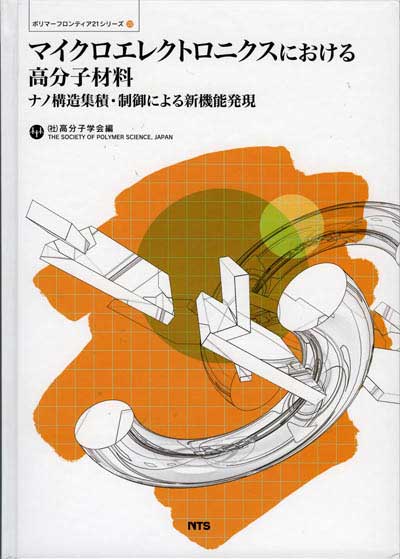 | |
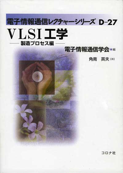
| 13. | 「VLSI工学-製造プロセス編-」, 電子情報通信学会編, 角南英夫著, 204頁, (株)コロナ社, 2006年8月。 → 目次 "VLSI-Fabrication Process," IEICE, H. Sunami, 204 pagers, Corona Pub. Co., Aug. 2006.→ contents |
 | |
| 14. | 「2007半導体テクノロジー大全」, Electronic Journal別冊,
角南英夫共著, 「キャパシタ形成技術総論、スタックトキャパシタ形成技術」, pp. 369-375, 電子ジャーナル社, 2007年。
"2007Semiconductor Technology Outlook," Electronic Journal Supplement, H. Sunami (coauthor), "Capacitor technology," pp. 369-375, Electronic Journal Pub. Co., 2007. |  | |
| 15. | 「超大規模集成電路ー基礎・設計・製造工程」, 電子情報通信学会編, 岩田穆、角南英夫共著, 309頁, (株)科学出版社、2008年1月。
"VLSI-design & process," (Ed. : IEICE), A. Iwata & H. Sunami, 309 pages, Science Pub.(china), Jan. 2008. | 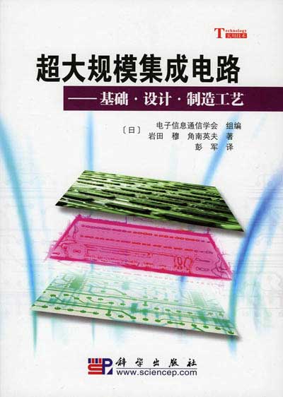 | |
| 16. | 「技術者のための特許事始ー半導体技術を中心としてー」, 角南英夫著, 149頁,コロナ社, 2008年1月。 → 目次 "Patent Application Guide for Engineers," H. Sunami, 149 pages, Corona Pub. Co., Jan 2008. |  | |
| 17. | 「半導体メモリ」, 角南英夫著, 196頁, コロナ社, 2008年8月。→
目次 "Semiconductor Memory," H. Sunami, 196 pages, Corona Pub. Co., Aug. 2008. → contents | 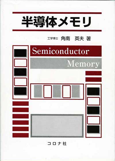 | |
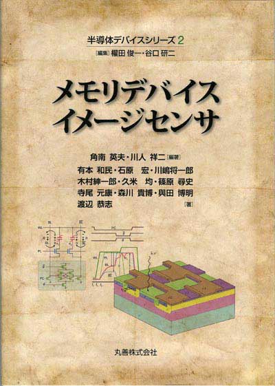
| 18. | 「メモリデバイス・
イメージセンサ」, 角南英夫・川人祥二編著, 292頁, 丸善, 2009年12月。 → 目次 "Memory Device and Image Sensor," H. Sunami (co-author) and S. kawahito, 292 pages, Maruzen, December 2009. |
 | |
| 19. | 「Solid State Circuits Technologies」,
角南英夫著, "Dimension Increase in Metal-Oxide-Semiconductor Memories and Transistors,"
1-26頁, In-Tech, 2009年12月。
"Solid State Circuits Technologies," H. Sunami (co-author), " Dimension Increase in Metal-Oxide-Semiconductor Memories and Transistors," 1-26 pages, In-Tech, Dec. 2009. |
| |
学術論文 / Technical Journals
- M. Kumagawa, H. Sunami, T. Terasaki, and J. Nishizawa, “Epitaxial Growth with Light Irradiation,” Japan. J. Appl. Phys., Vol. 7, No. 11, pp. 1331-1341, 1968.
- H. Sunami, T. Terasaki, N. Miyamoto, and J. Nishizawa, “Surface Orientation Effect of the Shadow of the Stacking Fault, ” J. Appl. Phys., Vol. 40, No. 11, pp. 4671-4673, 1969.
- H. Sunami, Y. Itoh, and K. Satoh, “Stress and Thermal Expansion Coefficient of Chemica1-Vapor-Deposited Glass Films,” J. Appl. Phys. Vol. 41, No. 13, pp. 5115-5117, 1970.
- M. Tamura and H. Sunami, “Generation of Dislocations Induced by Chemical Vapor Deposited Si3N4 Films on Silicon, ” Japan. J. Appl. Phys. Vol. 11, No. 8, pp. 1097-1105, 1972.
- H. Sunami, Y. Kamigaki, and Y. Itoh, “A Charge Transfer Model in CCD and the Experimental Verification,” Trans. Inst. Electronics Comm. Engrs, Japan, Vol. 55, No. 11, pp. 26-27, 1972.
- Hideo Sunami, Yoshiaki Kamigaki, and Yokichi Itoh, "Charge Transfer Model of CCD and Its Experimental Verification, " (in Japanese) IEICE(C), Vol. 55-C, No. 11, pp. 586-593, 1972 (角南英夫, 神垣良昭, 伊藤容吉, “CCDの電荷移送モデルとその実験的確証,” 信学論(C), 第55-C巻, 第11号, 586-593頁, 1972).
- Y. Kamigaki, H. Sunami, and Y. Itoh, “Bias Charge Optimization of High Speed CCD Operation,” Supplement to J. Japan Soc. Appl. Phys., Vol. 42, pp. 201-209, 1973.
- I. Takemoto, H. Sunami, S. Ohba, M. Aoki, and M. Kubo, “Bulk Charge-Transfer Device,” Supplement to J. Japan Soc. App. Phys., Vol. 43, No. 8, pp. 264-268, 1974.
- P. E. Gregory, P. W. Chye, H. Sunami, and W. E. Spicer, “The oxidation of Cs-uv photoemission studies, ” J. Appl. Phys., Vol. 46, No. 8, pp. 3525-3529, 1975.
- P. W. Chye, T. Sukegawa, I. A. Babalola, H. Sunami, P. Gregory, and W. E. Spicer, “Surface and interface states of GaSb:A photoemission study, ” Phys. Rev. B, Vol. 15, No. 4, pp. 2118-2126, 1977.
- T. Matsuzawa, H. Sunami, and N. Hashimoto, “Analysis of Superposition Errors in Wafer Fabrication,” Microelectron. Reliab., Vol. 16, pp. 173-176, 1977.
- H. Sunami, “Thermal Oxidation of Phosphorus Doped Polycrystalline Silicon in Wet Oxygen,” J. Electrochem. Soc., Vol. 125, No. 6, pp. 892-897, 1978.
- H. Sunami and M. Koyanagi, “Selective Oxide Coating of Silicon Gate (SELOCS),” Supplement to Japan. J. Appl. Phys., Vol. 18-1, pp. 255-260, 1979.
- M. Koyanagi, H. Sunami, and N. Hashimoto, “Novel High Density, Stacked Capacitor MOS RAM,” Supplement to Japan. J. Appl. Phys., Vol. 18-1, pp. 35-42, 1979.
- H. Sunami, M. Koyanagi, and T. Hashimoto, “Intermediate Oxide Formation in Double Polysilicon Gate MOS Structure,” J. Electrochem. Soc., Vol. 127, No. 11, pp. 2499-2506, 1980.
- H. Sunami, Y. Wada, and N. Hashimoto, “Experimental Characterization of MOST‘s Scaled Down to the 1?m Level,” Microelectron. Reliab., Vol. 20, No. 6, pp. 803-822, 1980.
- Y. Wada, H. Sunami, and N. Hashimoto, “Electrical Testing for Process Evaluations,” Microelectron. Reliab., Vol. 21, No. 2, pp. 159-163, 1981.
- H. Sunami, K. Shimohigashi, and N. Hashimoto, “Characterization of A Buried Channel Graded-Drain with Punchthrough Stopper (BGP) NMOS Device,” IEEE Trans. Electron Devices, Vol. ED-29, No. 4 , pp. 607-610, 1982.
- K. Itoh and H. Sunami, “High Density One-Device Dynamic MOS Memory Cells,” IEE Proc. 130, Pt. I, No. 3, pp. 127-135, 1983.
- H. Sunami, T. Kure, N. Hashimoto, K. Itoh, T. Toyabe, and S. Asai, “A Corrugated Capacitor Cell (CCC) for Megabit Dynamic MOS Memories,” IEEE Electron Device Lett., Vol. EDL-4, No. 4, pp. 90-91, 1983.
- H. Sunami, K. Shimohigashi, and N. Hashimoto, “An Optically Defined 1.3?m NMOS Ring Oscillator,” IEEE Electron Device Lett., Vol. EDL-4, No. 9, pp. 311-313, 1983.
- H. Sunami, T. Kure, N. Hashimoto, K. Itoh, T. Toyabe, and S. Asai, “A Corrugated Capacitor Cell (CCC),” IEEE Trans. Electron Devices, Vol. ED-31, No. 6, pp. 746-753, 1984 (recipient of 1984 IEEE Paul Rppaport Award).
- H. Sunami, Y. Kawamoto, K. Shimohigashi, and N. Hashimoto, “An Improved Planar Isolation with Buried-Channel MOSFET’s,” Microelectron. Reliab., Vol. 24, No. 3, pp. 555-577, 1984.
- K. Miyake, S. Kimura, T. Warabisako, H. Sunami, and T. Tokuyama, “Microwave plasma stream transport system for low temperature plasma oxidation,” J. Vac. Sci. Tech. A, Vol. 2, No. 2, Part 1, pp. 496-499, 1984.
- R. Hori, K. Itoh, J. Etoh, S. Asai, N. Hashimoto, K. Yagi, and H. Sunami, “An experimental 1Mbit DRAM based on high S/N design,” IEEE J. Solid State Circuits, Vol. SC-19, No. 5, pp. 634-640, 1984.
- K. Yamaguchi, R. Nishimura, T. Hagiwara, and H. Sunami, “Two-Dimensional Numerical Model of Memory Devices with a Corrugated Capacitor Cell (CCC) Structure,” IEEE Trans. Electron Devices, Vol. ED-32, No. 2, pp. 282-289, 1985.
- S. Kimura, E. Murakami, K. Miyake, T. Warabisako, H. Sunami, and T. Tokuyama, “Low Temperature Oxidation of Silicon in a Microwave-Discharged Oxygen Plasma,” J. Electrochem. Soc., Vol. 132, No. 6, pp. 1460-1466, 1985.
- H. Sunami, T. Kure, K. Yagi, K. Yamaguchi, and S. Shimizu, “Scaling Consideration and Dielectric Breakdown Improvement of Corrugated Capacitor Cell (CCC) for Future dRAM,” IEEE Trans. Electron Devices, Vol. ED-32, No. 2, pp. 296-303, 1985.
- M. Moniwa, M. Miyao, R. Tsuchiyama, A. Ishizaka, M. Ichikawa, H. Sunami, and T. Tokuyama, “Preferential nucleation along SiO2 steps in amorphous Si,” Appl. Phys. Lett., Vol. 47, No. 2, pp. 113-115, 1985.
- M. Ohkura, M. Ichikawa, M. Miyao, H. Sunami, and T. Tokuyama, “Two-Dimensional Dynamic Numerical Simulation of an SOI Formation Process in Laser-Induced Seeded Lateral Growth,” IEEE Trans. Electron Devices, Vol. ED-32, No. 7, pp. 1347-1352, 1985.
- T. Matsuzawa, T. Ito, M. Tanuma, N. Hasegawa, and H. Sunami, “A Three Dimensional Photoresist Image Simulator : TRIPS-I,” IEEE Electron Device Lett., Vol. EDL-6, No. 8, pp. 416-418, 1985.
- S.-I. Kimura, E. Murakami, T. Warabisako, H. Sunami, anfd T. Tokuyama, “Low-Teperature Fabrication of MOSFET’s Utilizing a Microwave-Exicited Plasma Oxidation Technique,” IEEE Electron Device Lett., Vol. EDL-7, No. 1, pp. 38-40, 1986.
- T. Kure, T. Komoda, H. Sunami, S. Okazaki, and T. Hayashida, “EXAD: A Novel Electron-Beam X-ray Absorption Method of Nondestructive Depth Measurement for Silicon Trenches,” IEEE Electron Device Lett., Vol. EDL-7, No. 12, pp. 703-704, 1986.
- S. Yamamoto, T. Kure, H. Ohgo, T. Matsuzawa, S. Tachi, and H. Sunami, “A Two-Dimensional Etching Profile Simulator : ESPRIT,” IEEE Trans. Computer-Aided Design, Vol. CAD-6, No. 3, pp. 417-422, 1987.
- A. Moniwa, T. Matsuzawa, T. Ito, and H. Sunami, “A Three-Dimensional Photoresist Imaging Process Simulator for Strong Standing-Wave Effect Environment,” IEEE Trans. Compute-Aided Design, Vol. CAD-6, No. 3, pp. 431-438, 1987.
- H. Ohgo, Y. Takano, A. Moniwa, S. Yamamoto, Y. Sakai, H. Masuda, and H. Sunami, “A Two-Dimensional Integrated Process Simulator:SPIRIT-I,” IEEE Trans. Computer-Aided Design, Vol. CAD-6, No. 3, pp. 439-445, 1987.
- T. Matsuzawa, A. Moniwa, N. Hasegawa and H. Sunami, “Two Dimensional Simulation of Photolithography on Reflective Stepped Surface,” IEEE Trans. Computer-Aided Design, Vol. CAD-6, No.3, pp.446-451, 1987.
- S. Kimura, E. Murakami, T. Warabisako, E. Mitani, and H. Sunami, “An 18O study of oxygen exchange phenomena during microwave-discharge plasma oxidation of silicon,” J. Appl. Phys., Vol. 63, No. 9, pp.4655-4660, 1988.
- T. Kaga, Y. Kawamoto, T. Kure, Y. Nakagome, H. Aoki, H. Sunami, T. Makino, N. Ohki, and K. Itoh, “Half-Vcc Sheath-Plate Capacitor DRAM Cell with Self-Aligned Buried Plate Wiring,” IEEE Trans. Electron Devices, Vol. 35, No. 8, pp. 1257-1263, 1988.
- M. Aoki, Y. Nakagome, M. Horiguchi, H. Tanaka, S. Ikenaga, J. Etoh, Y. Kawamoto, S. Kimura, E. Takeda, H. Sunami, and K. Itoh, “A 60-ns l6-Mbit CMOS DRAM with a Transposed Data-Line Structure,” IEEE J. Solid State Circuits, Vol. 23, No. 5, pp. 1113-1119, 1988.
- M. Ohkura, K. Kusukawa, and H. Sunami, “Beam Induced Seeded Lateral Epitaxy with Suppressed Impurity Diffusion for a Three-Dimensional DRAM Cell Fabrication,” IEEE Trans. Electron Devices, Vol. 36, No. 2, pp. 333-339, 1989.
- S. Kimura, Y. Kawamoto, T. Kure, N. Hasegawa, T. Kisu, J. Etoh, H. Aoki, E. Takeda, H. Sunami, and K. Itoh, “A Diagonal Active-Area Stacked Capacitor DRAM Cell with Storage Capacitor on Bit Line,” IEEE Trans. Electron Devices, Vol. 37, No. 3, pp. 737-743, 1990.
- Y. Takano, M. Ohgo, S. Yamamoto, and H. Sunami, “A versatile two-dimensional ion implantation simulator incorporated in an integrated process simulation system,” Microelectronic Engineering, Vol. 14, pp. 13-22, 1991.
- K. Itoh, H. Sunami, K. Nakazato, and M. Horiguchi, “Pathways to DRAM Design and Technology for the 21st Century,” the 193rd Electrochemical Society Spring Meeting, Abs. No. 303, San Diego, California, May 3-8, 1998; Proceedings of the 8th Internat. Symp. Silicon Materials Science and Technology, Volume 98-1, pp. 350-369, 1998.
- (Hideo Sunami and Michio Suzuki, "Next generation integrated circuits fabrication line - future perspective of devicesand 300-mm in diameter fabrication line," (in Japanese), Aerosol Research, Vol. 14, No. 1, pp. 11-18, 1999 (角南英夫, 鈴木道夫, 「次世代集積回路と製造ライン - 今後のデバイス展望と300mmウェハ製造ラインの動向 - 」,エアロゾル研究, 第14巻, 第1号, pp. 11-18, 1999).
- A. Nakajima, T. Yoshimoto, T. Kidera, K. Obata, S. Yokoyama, H. Sunami, and M. Hirose, “Atomic-layer-deposited silicon-nitride/SiO2 stacked gate dielectriocs for highly reliable p-metal-oxide-semiconductor field-effect transistors,” Appl. Phys. Lett., Vol. 77, No. 18, pp. 2855-2857, 30 October 2000.
- A. Nakajima, T. Yoshimoto, T. Kidera, K. Obata, S. Yokoyama, H. Sunami, and M. Hirose, “Characterization of atomic-layer-deposited silicon nitride/SiO2 stacked gate dielectrics for highly reliable p-metal-oxide-semiconductor field-effect transistors,” J. Vac. Sci. Tech. B, Vol. 19, pp. 1138-1143, 2001.
- Shin Yokoyama, Takenobu Yoshino, Kentaro Shibahara, Anri Nakajima, Takamaro Kikkawa, Hideo Sunami, and Quiz D. M. Khosru, "Influence of preservation ambient to MOS device characteristics," (in Japanese), Aerosol Research, Vol. 17, No. 2, , pp. 96-104, 2002 (横山新, 吉野雄信,芝原健太郎,中島安理,吉川公麿,角南英夫, Quiz D. M. Khosru, “ウェハ保管環境のMOSデバイス特性への影響,” エアロゾル研究, 第17巻, 第2号, pp. 96-104, 2002) .
- T. Furukawa, H. Yamashita, and H. Sunami, “A Proposal of Corrugated-Channel Transistor (CCT) with Vertically-Formed Channels for Area-Conscious Applications,” Jpn. J. Appl. Phys., Vol. 42, Part 1, No. 4B, pp. 2067-2072, April 2003.
- A. Takase, T. Kidera, and H. Sunami, “Field-Shield Trench Isolation with Self-Aligned Field Oxide,” Jpn. J. Appl. Phys., Vol. 42, Part 1, No. 4B, pp. 2100-2105, April 2003.
- Hideo Sunami, "ULSI perspective and expectations to high polymer materials," (in Japanese), Vol. 52, No. 8, pp. 546-550、2003 (角南英夫,「ULSIの将来展望と高分子材料への期待 」, 高分子, 第52巻, 8月号, pp. 546-550、2003).
- Q. D. M. Khosru, S. Yokoyama, A. Nakajima, K. Shibahara, T. Kikkawa, H. Sunami, and T. Yoshino, “Organic Contamination Dependence of Process-Induced Interface Trap Generation in Ultrathin Oxide Metal Oxide Semiconductor Transistors,” Jpn. J. Appl. Phys., Vol 42, Part 2, No. 12A, pp. L1429-L1432, 1 December 2003.
- H. Sunami, T. Furukawa, and T. Masuda, “A Three-Dimensional MOS Transistor Formation Technique with Crystallographic Orientation-Dependent TMAH Etchant,” SENSORS and ACTUATORS A: PHYSICAL, A111, pp. 310-316, 2004.
- A. Katakami, K. Kobayashi, and H. Sunami, “A High-Aspect Ratio Silicon Gate Formation Technique for Beam-Channel MOS Transistor with Impurity-Enhanced Oxidation,” Jpn. J. Appl. Phys., Vol. 43, No. 4B, pp. 2145-2150, April 2004.
- K. Kobayashi, T. Eto, K. Okuyama, K. Shibahara, and H. Sunami, "Application of Arsenic Plasma Doping in Three-Dimensional MOS Transistors and the Doping Profile Evaluation," Jpn. J. Appl. Phys., Vol. 44, No. 4B, pp. 2273-2278, April 2005.
- H. Sunami S. Matsumura, K. Yoshikawa, and K. Okuyama, "High-aspect-ratio structure formation techniques for three-dimensional metal-oxide-semiconductor transistors," Microelectronic Engineering, Vol. 83, pp. 1740-1744, 2006 .
- T. Tabei, K. Maeda, S. Yokoyama, and H. Sunami, "Fabrication of Spin-Coated Optical Waveguides for Optically Interconnected LSI and Influence of Fabrication Process on Underlying Metal-Oxide-Semiconductor Capacitors," Jpn. J. Appl. Phys., Vol. 45, No. 4B, pp. 3498-3503, 2006.
- Shunpei Matsumura, Atsushi Sugimura, Kiyoshi Okuyama, and Hideo Sunami, “Anomalous Whisker Generation in Ni-Silicided Source and Drain for Three-Dimensional Beam-Channel MOS Transistor on SOI Substrate,” Proc. of Advanced Metallization Conference 2006, pp. 631-635, ADMETA, 2007.
- Kei Kobayashi, Kiyoshi Okuyama, and Hideo Sunami, “Plasma doping induced damages associated with source/drain fomrmation in three-dimensional beam-channel MOS transistor,” Microelectronic Engineering, Vol. 84, pp. 1631-1634, 2007.
- K. Okuyama, K. Yoshikawa, and H. Sunami, “Control of Subthreshold-Characteristics of Narrow- channel SOI nMOS Transistor Utilized Additional Side Gate Electrodes,” Jpn. J. Appl. Phys., Vol. 46, No. 4B, pp. 2050-2053, 2007.
- Hideo Sunami, “The Role of the Trench Capacitor in DRAM Innovation,” IEEE SSCS News, Vol. 13, No.1, pp. 42-44, Winter 2008.
- Kiyoshi Okuyama, Atsushi Sugimura, and Hideo Sunami, “Optimized Silicidation Technique for Source and Drain of Fin-Type Field-Effect Transistor,” Jpn. J. Appl. Phys., Vol. 47, No. 4, pp. 2407-2409, 2008.
- Tomoki Hirata, Kenta Kajikawa, Tetsuo Tabei, and Hideo Sunami, “Proposal of a Metal-Oxide- Semiconductor Silicon Optical Modulator Based on Inversion-Carrier Absorption,” Jpn. J. Appl. Phys., Vol. 47, No. 4, pp. 2906-2909, 2008.
- Kenta Kajikawa, Tetsuo Tabei, and Hideo Sunami, “An infrared Silicon Optical Modulator of Metal-Oxide-Semiconductor Capacitor Based on Accumulation-Carrier Absorption,” Jpn. J. Appl. Phys., Vol. 48, No. 4, pp. 04C107-1-4, 2009.
- Atsushi Sugimura, Kiyoshi Okumura, Hideo Sunami, “Proposal of a Vertical-Channel Metal Oxide Semiconductor Field-Effect Transistor with Entirely Oxidized Silicon Beam Isolation,” Jpn. J. Appl. Phys., Vol. 48, No. 4, pp. 04C049-1-4, 2009.
- Tetsuo Tabei, Tomoki Hirata, Kenta Kajikawa, and Hideo Sunami, “Potentiality of Metal-Oxide-Semiconductor Silicon Optical Modulator Based on Free Carrier Absorption,” Jpn. J. Appl. Phys., Vol. 48, No. 4, pp. 114501-1-7, 2009.
- T. Kudo, T. Kasama, S. Yokoyama, T. Kikkawa, H. Sunami, T. Ishikawa, T. Ikeda, Y. Hata, M. Suzuki, S. Tokonami, K. Okuyama, T. Tabei, K. Ohkura, Y. Kayaba, Y. Tanushi, Y. Amemiya, Y. Cho, T. Monzen, Y. Murakami, A. Kuroda, A. Nakajima, “Fabrication of Si Nanowire FieldEffect Transistor for Highly Sensitive, LabelFree Biosensing,” Jpn. J. App. Phys. 48, No. 6, (2009) pp. 06FJ04-1-4.
- Yoichi Ashida, Kiyoshi Okuyama, and Hideo Sunami, "Preliminary characterization of a metal-gas-semiconductor field-effect transistor (MGSFET) proposed," Microelectronic Engineering, Vol. 88, pp. 213-217, 2011.
国際学会発表 / International Conference Presentation
- H. Sunami, Y. Itoh, and K. Sato, “Stress and Thermal Expansion Coefficient of Chemical Vapor Deposited Glass Films,” Technical Digest of Symp. on Thermal Expansion of Solids, p. 45, Santa Fe, New Mexico, June 10-12, 1970.
- H. Sunami, Y. Itoh, and K. Sato, “Low Stress CVD Glass Films in Multi-Level Interconnection,” Proceedings of the 2nd Conference on Solid State Devices, Tokyo, Sept. 1970: Supplement to J. Japan Soc. Appl. Phys, Vol. 40, No. 8, pp. 67-70, 1971.
- Y. Kamigaki, H. Sunami, and Y. Itoh, “Bias Charge Optimization of High Speed CCD Operation,” Proceedings of the 4th Conference on Solid State Devices, Abs. No. 6-4, Tokyo, Aug. 30-31, 1972.
- I. Takemoto, H. Sunami, S. Ohba, M. Aoki, and M. Kubo, “Bulk Charge-Transfer Device,” Proceedings of the 5th Conference on Solid State Devices, Abs. No. 7-2, Tokyo, Aug 30-31, 1973.
- H. Sunami and M. Koyanagi, “Selective Oxide Coating of Silicon Gate (SELOCS) ,”? Proceedings of the 10th Conf. on Solid State Devices, pp. 67-68, Tokyo, Aug. 29-30, 1978.
- M. Koyanagi, H. Sunami, N. Hashimoto, and M. Ashikawa, “Novel High Density, Stacked Capacitor MOS RAM,” Technical Digest of IEEE Internat. Electron Devices Meeting, pp. 348-358, Washing-ton, D. C., Dec. 4-6, 1978.
- H. Sunami, K. Shimohigashi, and N. Hashimoto, “Characterization of A Buried-Channel Graded-Drain with Punchthrough Stopper(BGP) MOS Device,” Technical Digest of Symp. on VLSI Technology, pp. 20-21, Hawaii, Sept. 1981.
- M. Koyanagi, T. Kamiyama, H. Sunami, and N. Hashimoto, “Electrical Properties of SiO2 Films in Double-Level Poly-Si Structures,” Extended Abstracts of the 155th Electrochemical Society Spring Meeting, Vol. 7-l, Abs. No. 87, pp. 225-227, May 6-11, 1979.
- K. Itoh and H. Sunami, “High Density Memory Cell Structure,” Technical Digest of Symp. on VLSI Technology, pp. 48-49, Hawaii, Sept. 1981.
- H. Sunami, T. Kure, N. Hashimoto, K. Itoh, T. Toyabe, and S. Asai, “A Corrugated Capacitor Cell (CCC) for Megabit Dynamic MOS Memories,” Technical Digest of IEEE Internat. Electron Devices Meeting, pp. 806-808, San Francisco, Dec. 13-15, 1982.
- K. Miyake, S. Kimura, T. Warabisako, H. Sunami, and T. Tokuyama, “Microwave Plasma Stream Transport System for Photo Assisted Plasma Oxidation of Silicon Surfaces,” Proceedings of Internat. Ion Engineering Congress-ISIAT ‘83 and IPAT ‘83, pp. 915-920, Kyoto, 1983.
- Y. Wada, H. Sunami, N. Yamamoto, Y. Kawamoto, T. Mizutani, K. Yagi, Y. Homma, N. Hashimoto, and S. Asai, “A 1.3?m N-MOS VLSI Technology,”? Technical Digest of IEEE Internat. Electron Devices Meeting, pp. 323-325, Washington, Dec. 5-7, 1983.
- K. Yagi, H. Tamura, T. Kure, H. Sunami, N. Hashimoto, and S. Asai, “Improvement of Breakdown Characteristics of Storage Capacitor Insulating Materials,” Abstracts of Electronic Materials Conference, pp. 51-52, Vermont, 1983.
- H. Sunami, T. Kure, K. Yagi, K. Yamaguchi, and S. Shimizu, “Scaling Consideration and Dielectric-Breakdown Improvement of Corrugated Capacitor Cell (CCC) for Future dRAM” Technical Digest of IEEE Internat. Electron Devices Meeting, pp. 232-235, San Francisco, Dec. 9-12, 1984.
- K. Itoh, R. Hori, J. Etoh, S. Asai, N. Hashimoto, K. Yagi, and H. Sunami, “An Experimental 1Mbit DRAM with On-Chip Voltage Limiter,” Technical Digest of IEEE Internat. Solid-State Circuits Conf., pp. 282-283, San Francisco, Feb. 22-24, 1984.
- S. Kimura, E. Murakami, K. Miyake, T. Warabisako, and H. Sunami, “Low Temperature Oxidation of Silicon by Discharged Oxygen Plasma,” Proceedings of Internat. Conf. on Solid State Devices and Materials, Abs. No. A-11-3, pp. 467-470, Koube, Aug. 30-Sept. 1, 1984.
- H. Ohkura, H. Ichikawa, M. Miyao, H. Sunami, and T. Tokuyama, “Dynamic Numerical Simulation of Melting and Resolidification Process in SOI Formation by Seeded Lateral Epitaxy.” Proceedings of Internat. Conf. on Solid State Devices and Materials, Abs. No. B-9-2, pp. 503-506, Koube, Aug. 30-Sept. 1, 1984.
- M. Miyao, M. Moniwa, M. Ichikawa, A. Ishizaka, T. Doi, H. Sunami, and T. Tokuyama, “Nucleation Control and Epitaxial Alignment in Silicon On Insulator Structure during Solid Phase Growth,” Proceedings of Internat. Conf. on Solid State Devices and Materials, Abs. No. B-9-4, pp. 511-514, Koube, Aug. 30-Sept. 1, 1984.
- M. Miyao, M. Moniwa, T. Warabisako, H. Sunami, and T. Tokuyama, “Formation of Si-On-Insulator Structure under Solid Phase Growth,” Proceedings of Mat. Res. Soc. Symp., Vol. 35, pp. 705-709, Boston, Dec. 2-4, 1985.
- H. Sunami and S. Asai, “Trends in Megabit dRAM’ s (Invited),” Technical Digest of the 2nd International Symp. on VLSI Technology, Systems and Applications, pp. 4-8, Taipei, May 8-10, 1985.
- H. Sunami, “Cell Structures for Future dRAM‘s (Invited),” Technical Digest of IEEE Internat. Electron Devices Meeting, pp. 694-697, Washington, D. C., Dec. 1-4, 1985.
- K. Yamaguchi, R. Nishimura, T. Hagiwara, and H. Sunami, “Theoretical Characterization of Corrugated Capacitor Cell(CCC) Structure Devices by a Time-Dependent Numerical Analysis in Two Dimensions and Three-Dimensional DC Simulation,” Proceedings of 1985 Internat. Symposium on Circuits and Systems (ISCAS ヤ85), Vol. 2 of 3, pp. 431-432, Kyoto, June 5-7, 1985.
- M. Ohkura, K. Kusukawa, H. Sunami, and T. Tokuyama, “Orientation Controlled SOI by Line Shaped Laser Beam Seeded Lateral Epitaxy for CMOS Stacking,” Extended Abstracts of the 17th Conf. on Solid State Devices and Materials , pp. 143-146, Tokyo, Aug. 25-27, 1985.
- E. Takeda, K. Takeuchi, A. Hiraiwa, T. Toyabe, H. Sunami, and K. Itoh, “Three Dimensional Leakage Current in Corrugated Capacitor Cells,” Extended Abstracts of the 17th Conf. on Solid State Devices and Materials, pp. 37-40, Tokyo, Aug. 25-27, 1985.
- M. Ohkura, K. Kusukawa, H. Sunami, T. Hayashida, and T. Tokuyama, “A Three-Dimensional DRAM Cell of Stacked Switching-Transistor in SOI(SSS),” Technical Digest of IEEE Internat. Electron Devices Meeting, pp. 718-721, San Francisco, Dec. 9-12, 1985.
- S. Kimura, E. Murakami, T. Warabisako, E. Mitani, and H. Sunami, “Oxygen Exchange Phenomena in SiO2 During Microwave-Discharged Plasma Oxidation,” Abstracts of Fall Meeting of Materials Research Society Symposium, p. 112, Boston, Dec. 16, 1986.
- S. Kimura, Y. Kawamoto, N. Hasegawa, A. Hiraiwa, M. Horiguchi, H. Aoki, T. Kisu, and H. Sunami, “A 5.4 mm2 Stacked Capacitor DRAM Cell with 0.6mm Quadruple-Polysilicon Gate Technology,” Extended Abstracts of the 19th Conf. Solid-State Devices and Materials, pp. 19-22, Tokyo, Aug. 25-27, 1987.
- T. Kaga, Y. Kawamoto, T. Kure, Y. Nakagome, M. Aoki, T. Makino, and H. Sunami, “A 5.4 mm2 Sheath-Plate-Capacitor DRAM Cell with Self-Aligned Storage Node Insulation,” Extended Abstracts of the 19th Conf. Solid-State Devices and Materials, pp. 15-18, Tokyo, Aug. 25-27, 1987.
- T. Kure, T. Komoda, M. Noguchi, H. Sunami, and T. Hayashida, “Depth Measurement Techniques for Silicon Trenches,” Extended Abstracts of the 19th Conf. Solid-State Devices and Materials, pp. 307-310, Tokyo, Aug. 25-27, 1987.
- T. Kaga, Y. Kawamoto, T. Kure, Y. Nakagome, H. Aoki, H. Sunami, and K. Itoh, “A 4.2 mm2 Half-Vcc Sheath-Plate Capacitor DRAM Cell with Self-Aligned Buried Wiring,” Technical Digest of IEEE Internat. Electron Devices Meeting, pp. 332-335, Washington, D. C., Dec. 6-9, 1987.
- H. Sunami, T. Matsuzawa, M. Ohgo, and S. Yamamoto, “Computer-Aided Design of ULSI Processing Prior to Fabrication,” Extended Abstracts of the 171st Electrochem. Soc. Spring Meeting, Abs. No. 202, p. 291, Philadelphia, Pennsylvania, May 10-15, 1987 and Proceedings of the First International Symp. on Ultra Large Scale Integration Science and Technology, ULSI Science and Technology/1987, The Electrochemical Society, pp. 652-659.
- T. Kisu, S. Kimura, T. Kure, J. Yugami, A. Hiraiwa, Y. Kawamoto, M. Aoki, and H. Sunami, “A Novel Capacitance Enlargement Structure Using a Double-Stacked Storage Node in STC DRAM Cell,” Extended Abstracts of the 20th Conf. Solid State Devices and Materials, pp. 581-584, Tokyo, Aug. 24-26, 1988.
- H. Sunami, “Metrology for Trench Control,” 1988 Symposium on VLSI Technology, Special Workshop, San Diego, May 10, 1988.
- Y. Kawamoto, S. Kimura, N. Hasegawa, A. Hiraiwa, T. Kure, T. Nishida, M. Aoki, H. Sunami, and K. Itoh, “A Half Micron Technology for An Experimental 16 bit DRAM Using i-Line Stepper,” Symp. VLSI Technology Tech. Dig., pp. 17-18, May 10-13, San Diego, 1988.
- H. Sunami, “Technology Trends in Dynamic RAM‘s:64Mb and Beyond (Invited),” the 21st Semiconductor Interface Specialists Conference, Abs. No. I-1, San Diego, Dec. 6-8, 1990.
- K. Itoh, H. Sunami, K. Nakazato, and M. Horiguchi, “Pathways to DRAM Design and Technology for????? the 21st Century,” the 193rd Electrochemical Society Spring Meeting, Abs. No. 303, San Diego, California, May 3-8, 1998.
- H. Sunami, “Pathways to Giga-scale Electronics for the 21st Century,” Seventh Hitachi Cambridge Seminar, Cambridge, July 6, 1998.
- T. Yoshino, S. Yokoyama, T. Suzuki, T. Fujii, K. Shibahara, A. Nakajima, T. Kikkawa, H. Sunami, and Q.D.M. Khosru, “Influence of Organic Contamination on Reliability and Trap Generation in MOS,” Extend. Abst. of the Int. Conf. on Solid State Devices and Materials (Tokyo, 2001), pp. 176-177, 2001.
- H. Sunami, T. Furukawa, and T. Masuda, “Orientation-Dependent Anisotropic TMAH Etchant Applied to 3-D Silicon Nanostructure Formation,” Proc. Pacific Rim Workshop on Transducers and Micro/nano Technologies, pp. 367-372, Xiamen, July 22-24, 2002.
- T. Furukawa, H. Yamashita, and H. Sunami, “Corrugated-Channel Transistor (CCT) for Area-Conscious Applications,” Extended Abstracts of International Symp. on Solid State Devices and Materials, Abs. No. A-3-2, pp. 139-140, Nagoya, Sept. 17-19, 2002.
- A. Takase, T. Kidera, and H. Sunami, “Field-Shield Trench Isolation with Self-Aligned Field Oxide,” Extended Abstracts of International Symp. on Solid State Devices and Materials, Abs. No. A-7-4, pp. 694-695, Nagoya, Sept. 17-19, 2002.
- A. Katakami, K. Kobayashi, and H. Sunami, “High-Aspect Ratio gate Formation of Beam-Channel MOS Transistor with Impurity-Enhanced oxidation of Silicon Gate,” Extended Abstracts of International Symp. on Solid State Devices and Materials, Abs. No. D-5-2, pp. 282-283, Tokyo, Sept. 16-18, 2003.
- K. Kobayashi, T. Eto, K. Okuyama, K. Shibahara, and H. Sunami, “An Impurity-Enhanced Oxidation Assisted Doping Profile Evaluation for Three-Dimensional and Vertical-Channel Transistors,” Extended Abstracts of International Symp. on Solid State Devices and Materials, Abs. No. B-6-3, pp. 208-209, Tokyo, Sept. 15-17, 2004.
- M. Kawai, K. Endo, T. Tabei, and H. Sunami, “An Experimental Analysis of 1.55-mm Infrared Light Propagation in Integrated SOI Structure,” Extended Abstracts of International Symp. on Solid State Devices and Materials, Abs. No. P7-1, pp. 556-557, Tokyo, Sept. 15-17, 2004.
- H. Sunami, K. Kobayashi, and S. Matsumura, “Integrated Power Transistor Application of Three- Dimensional Sidewall-Channel MOS Transistor (invited),” Proc. the 7th International Conference on Solid-State and Integrated-Circuit Technology (ICSICT 2004), Abs. No. A7.3, pp. 336-339, Beijin, China, Oct. 18-21, 2004.
- H. Sunami, “Recent Activities for Nano-device and Process Technology Development in the 21st COE: Nanoelectronics for Terabit Information Processing,” Tech. Dig. 2004 International Symposium on Nano Science and Technology, pp. 3-8, Tainan, Taiwan, Nov. 20-21, 2004.
- A. Iwata, M. Sasaki, T. Kikkawa, S. Kameda, H. Ando, K. Kimoto, D. Arizono, and H. Sunami, “A 3D Integration Scheme utilizing Wireless Interconnections for Implementing Hyper Brain,” ISSCC Tech. Dig., pp. 262-263, Feb. 2005.
- T. Tabei, K. Maeda, S. Yokoyama, and H. Sunami, “Fabrication of spin-coat optical waveguides for optically interconnected LSI and influence of fabrication process on lower layer MOS capacitors,” Extended Abstracts of International Symp. on Solid State Devices and Materials, Abs. No. E-4-4, pp. 332-333, Tokyo, Sept. 13-15, 2005.
- H. Sunami and K. Okuyama, “High-Aspect-Ratio Structure Formation Techniques for Three- Dimensional Metal-Oxide-Semiconductor Transistors,” Abstract of 31st International Conference on Micro- and Nano-Engineering, No. 11B_03, Sept. 19-22, Vienna, Austria, 2005.
- K. Okuyama, K. Yoshikawa, and H. Sunami, “Characterization of Subthreshold Behavior of Narrow-Channel SOI nMOSFET with Additional Side-Gate Electrodes,” Extended Abstracts of International Symp. on Solid State Devices and Materials, pp. 506-507, Tokyo, Sept. 13-15, 2006.
- Kei Kobayashi, Kiyoshi Okuyama, and Hideo Sunami, “Plasma-Doping Induced Damages Associated with Source/Drain Formation in Beam-Channel MOS Transistor on 1-mm Thick SOI Substrate,” Abstract of 32nd International Conference on Micro- and Nano-Engineering, pp. 493-494, Sept. 17-20, Barcelona, Spain, 2006.
- S. Matsumura, A. Sugimura, K. Okuyama, and H. Sunami, “Anomalous Whisker Generation in Ni-Silicided Source and Drain for Three-Dimensional Beam-Channel MOS Transistor on SOI Substrate,” Abstract of Advanced Metallization Conference, pp. 90-91, Sept. 25-27, Tokyo, 2006.
- K. Okuyama, K. Yoshikawa, and H. Sunami “Proposal of 3-Dimensional Independent Triple-Gate MOS Transist with Dynamic Current Control,” 14th International Symposium on VLSI Technology, Systems, and Applications (2007 VLSI-TSA), Hsinchu, Taiwan, April 23-25, 2007.
- Kiyoshi. Okuyama, Atsushi. Sugimura, and Hideo Sunami, “An Optimized Silicidation Technique for Source and Drain of FINFET,” Extended Abstracts of International Symp. on Solid State Devices and Materials, pp. 1044-1045, Tokyo, Sept. 19-21, 2007.
- Tomoki Hirata, Kenta Kajikawa, Tetsuo Tabei, and Hideo Sunami, “Proposal of a Silicon Optical Modulator Based on Inversion-Carrier Absorption,” Extended Abstracts of International Symp. on Solid State Devices and Materials, pp. 280-281, Tokyo, Sept. 19-21, 2007.
- Tetsuo Tabei, Tomoki Hirata, Kenta Kajikawa, and Hideo Sunami, “Potentiality of Silicon Optical Modulator Based on Free-Carrier Absorption,” Technical Digest of IEEE Internat. Electron Devices Meeting, pp. 1023-1026, Washington, D. C., Dec. 10-12, 2007.
- Hideo Sunami, “The invention and development of the first trench capacitor DRAM cell,” CMOS Emerging Technologies Workshop, Session 4, Vancouver, Canada, August 5-7, 2008.
- Youichi Ashida, Kiyoshi Okuyama, and Hideo Sunami, “Proposal of a metal-gas-semiconductor field-effect transistor, MGSFET with potential catastrophic-breakdown hardness,” Abstract of 34th International Conference on Micro and Nano Engineering, Abs. No. NED-P16, Athens, Greece, Sept. 15-18, 2008.
- Atsushi Sugimura, Kiyoshi Okuyama, and Hideo Sunami, “A Vertical-Channel Metal-Oxide- Semiconductor Field-Effect Transistor with Fully-Oxidized Silicon Beam Isolation,” Extended Abstracts of International Symp. on Solid State Devices and Materials, P-3-8, Tokyo, Sept. 23-26, 2008.
- Kenta Kajikawa, Tetsuo Tabei, and Hideo Sunami, “Silicon Optical Modulator Based on Accumulation-Carrier Absorption of Metal-Oxide-Semiconductor Capacitor Waveguide,” Extended Abstracts of International Symp. on Solid State Devices and Materials, Abs. No. E-2-2, Tokyo, Sept. 23-26, 2008.
- Hideo Sunami, “Development of three-dimensional MOS structures from trench-capacitor DRAM cell to pillar-type transistor,” Proc. the 9th International Conference on Solid-State and Integrated- Circuit Technology, pp. 853-856, Beijin, China, October 20-23, 2008.
- T. Tabei, K. Maeda, S. Yokoyama, and H. Sunami, “Monolithic Integaration of Si-Dot Light Emitting Diodes,” Extended Abstracts of International Symp. on Solid State Devices and Materials, Abs. No. I-2-d, Sendai, Oct. 7-9, 2009.
国内学会発表 / Domestic Conference Presentation
- 熊川征治、 角南英夫、西澤潤一、「気相成長法に於ける光照射の効旺と成長層の結晶性」、昭和41年度電気通信学会全国大会、予稿集No. S86、pp. 155-156、1966年.
- 角南英夫、熊川征治、西澤潤一、「唖相差顕微法及び多重干渉法を用いたシリコンエピタキシャル成長表蔓の観察」、電子通信学会創立50周年記念全国大会(昭和42年度) 、予稿集No. 777、1967年.
- 熊川征治、角南英夫、寺崎健、西澤潤一、「シリコンの気相成長における光照射の効旺と格子欠陥」電子通信学会半導体・トランジスタ研究会、資料No. SSD67-11(1967-08) 、pp. 1-15、1967年8月25日.
- 角南英夫、寺崎健、西澤潤一、「気相成長シリコン結晶中の積層欠陥」、日本学術振興会、薄膜第131委貝会、第38回研究会資料No. 185、pp. 5-14、1968年7月20日.
- 西澤潤一、熊川征治、角南英夫、「Si気相エピタキシヤル成長層における格子欠陥」、昭和43年電気四学会連合大会、予稿集No. S73、pp. 11-14、1968年.
- 角南英夫、寺崎健、宮本信雄、西澤潤一、「シリコンの気相成長層の構造欠陥」、電気学会、トランジスタ専門委員会資料、1969年1月27日.
- 角南英夫、寺崎健、宮木信雄、西澤潤一、「シリコンのエピタキシヤル層の構造欠陥」、電子通信学会半導体・トランジスタ研究会、資料No. SSD69-10(1969-06)、pp. 1-15、1969年6月26日.
- 伊藤容吉、角南英夫、神垣良昭、「Charge Transfer Characteristics in CCD」、日本学術振興会、薄膜第131委貫会、第57回研究会資料No. 307、pp. 1-3、1971年12月6日.
- 神垣良昭、角南英夫、伊藤容吉、「Charge Transfer Model in CCD (1) Theory」、1972年春季第19回応用物理学会関係連合講演会、予稿集No. 3a-C-3、p. 365、千葉大学、1972年4月3日.
- 伊藤容吉、角南英夫、高岡スミ子、神垣良昭、「Charge Transfer Model in CCD (1) Image Simulation」、1972年春季第19回応用物理学会関係連合講演会、予稿集No. 3a-C-5、p. 367、千葉大学、1972年4月3日.
- 伊藤容吉、神垣良昭、角南英夫、「CCDの画像処理シミユレーション」、テレビジョン学会、テレピジョン電子装置研究委員会資料、pp. 1-23、1973年3月7日.
- 神垣良昭、角南英夫、伊藤容吉、「CCDにおける信号電荷の再生」、1973年春季第20回応用物理学会関係連合講演会、予稿集No.29a-P-3、p. 237、慶応大学、東京、1973年3月28-31日.
- 角南英夫、伊藤容吉、佐藤喜久治、「多層配線集積回路の低応力ガラス絶縁膜」昭和45年度電子通信学会全国大会、予稿集No. 708、p. 767、1970年8月.
- 角南英夫、伊藤容吉、「半導体素子に用いられる薄膜の真性応力と熱膨張係数の測定法」、昭和46年電気学会全国大会、予稿集No. 1166、p. 577、徳島大学、1971年3月.
- 角南英夫、神垣良昭、伊藤容吉、「CCDによる電荷移送の動作実験」、1971年(昭和46年) 秋季第32回応用物理学会学術講演会、予稿集No. 1a -H-5、p. 158、大阪大学、大阪、1971年11月1日.
- 角南英夫、神垣良昭、伊藤容吉、「CCDの電荷移送機構」、電子通信学会半導体・トランジスタ研究会、資料No. SSD71-68(1972-02) 、pp. 1-14、1972年2月24日.
- 角南英夫、神垣良昭、伊藤容吉、「CCDにおける電荷移送モデル」、昭和47年電子通信学会全国大会、予稿集No. 976、p. 1048、東京、1972年3月.
- 角南英夫、神垣良昭、伊藤容吉、「n-チャネルCCDの基礎実験」、1973年春季第20回応用物理学会関係連合講演会、予稿集No. 29a-P-2、p. 236、慶応大学、東京、1973年3月28-31日.
- 角南英夫、神垣良昭、伊藤容吉、「CCD電荷移送のバイアス電荷効旺」、1975年春季第22回応用物理学会関係連合講演会、予稿集No. 2a-C-2、p. 39、千葉工業大学、千葉、1975年4月14日.
- 角南英夫、小柳光正、「シリコンゲートの選択酸化膜被覆技術(SELOCS) 」、電子通信学会半導体・トランジスタ研究会、資料No. SSD77-26、pp. 27-36、1977年8月24日.
- 角南英夫、「リン添加多結晶シリコンの熱酸化機構」、1978年秋季第39回応用物理学会学術講演会、予橋集、No. 5a-X-6、p. 433、近畿大学、大阪、1978年11月3-5日.
- 角南英夫、和田恭雄、橋本哲一、「短チャネル領域におけるMOSトランジスタの実効移動度」、1979年秋季第40回応用物理学会学術講演会、予稿集No. 1a-L-10、北海道大学、1979年9月30日-10月2日.
- 角南英夫、久禮得男、橋本哲一、伊藤清男、浅井彰二郎、「新ダイナミックメモリセル:CCC (Corrugated Capacitor Cell) 」、電気学会第6回半導体デバイス調査専門委員会、東京大学生産技術研究所、1983年2月l0日.
- 角南英夫、久禮得男、橋本哲一、伊藤清男、浅井彰二郎、「新ダイナミックメモリセル:CCC」、昭和58年度電子通信学会総合全国大会、予稿集No. S2-6、pp. 413-414、1983年4月2-4日.
- 大倉理、市川畠和、宮尾正信、角南英夫、「レーザー照射SOI形成の計算機シミユレーション」、1984年春季第31回応用物理学会関係連合講演会、予稿集No.31a -U-2、p. 443、明治大学、東京、1984年3月29日-4月2日.
- 楠川喜久雄、大倉理、宮尾正信、角南英夫、「レーザー照射SOI形成の下層構造への影響」、1984年春季第31回応用物理学会閲係連合講演会、予稿集No. 31p-U-10、p. 449、明治大学、東京、1984年3月29日-4月2日.
- 木村紳一郎、村上英一、蕨迫光紀、三宅潔、角南英夫、「有磁場マイクロ波プラズマによるシリコンの低温酸化(I) 」、1984年春季第31回応用物理学会関係連合講演会、予稿集No. 1p-U-1、p. 45、明治大学、東京、1984年3月29日-4月2日.
- 村上英一、末村紳一郎、三宅潔、蕨迫光紀、角南英夫、「有磁場マイクロ渡プラズマによるシリコンの低温酸化(II) 」、1984年春季第31回応用物理学会関係連合講演会、予稿集No. 1p-U-2、p. 455、明治大学、東京、1984年3月29日-4月2日.
- 山口憲、西村玲子、萩原隆且、角南英夫、「メガビット級d RAM用溝型キヤパシタの二次元過渡解析」、1984年秋季第45回応用物理学会学術講演会、予稿集No. 14a-A-10、p. 409、岡山大学、1984年10月12日-15日.25) 角南英夫、「d RAMの限界:太規模化を妨げる因子とブレークスルー」、 日本電子工業振興協会、電子デバイス講演会、機械振興会館、東京、1985年7月1日.
- 山口憲、西村玲子、萩原隆且、角南英夫、「溝型キャパシタセルの三次元動作解析」、第32回春季応用物理学会関係運合講演会、予稿集No. la-E-9、p. 551、青山学院大学、東京、1985年3月29日-4月l日.
- 木村紳一郎、村上英一、蕨追光紀、角南英夫、「マイクロ波ブラズマによるシリコンの低温酸化」、電気学会、プラズマ研究会資料No. EP-85-3、pp. 17-24、1985年6月18日.
- 竹内幹、武田英次、平岩篤、鳥谷部達、角南英夫、伊藤清男、「溝型キャパシタにおける三次元リーク電流」、昭和60年秋季第46回応用物理学会学術講演会、予稿集No. 4a-V-6、p. 422、京都大学、京都、1985年10月l日-4日.
- 角南英夫、「0.5mm時代のプロセス・デバイス」、昭和63年度電子情報通信学会春季全国大会特腹企画、エレクトロニクスグルーブ講習会「0.5mm ULSIテクノロジー」予稿集、pp. 25-34、早稲田大学、東京、1988年3月29日.
- 加賀徹、川本佳史、中込儀延、青木正和、角南英夫、牧野藤八、大木長斗司、伊藤清男、「ハーフVcc鞘プレート容裏型DRAMセル」、昭和63年度電子通信学会春季全国大会予稿集、p. 2-181、早稲田大学、東京、1988年3月28日-31日.
- 角南英夫、「シリコンデバイスの将来と関連基礎研究のあるべき姿について」、(財) 新機能素子研究開発協会、第1回超高集積素子研究委貰会講演会、東京、1989年4月17日.
- 角南英夫、「シリコンULSIの現状と将来」、電子情報通信学会講演会、富山大学、富山、1989年5月19日.
- 角南英夫、「ULSI時代のシリコンテクノロジー」、応用物理学会、第17回薄膜・表蔓物埋セミナー予稿集、p. 112、機械振興会館、東京、1989年7月19日.
- 角南英夫、「21世紀のDRAMメモリセル技術」、平成9年度電気学会、電子・情報・システム部門大会、予稿集、pp. 31-34、成蹊大学、東京、1997年8月28日.
- 高瀬明浩、角南英夫、「LSI素子分離におけるエッジ効果の低減」、第61回応用物理学会学術講演会、予稿集No. 5p-ZE-5、p. 782、北海道工業大学、札幌、2000年9月3日-9月7日.
- 古川智康、角南英夫、「ビームチャネルMOSFETによる赤外光スイッチの提案」、第61回応用物理学会学術講演会、予稿集No. 6p-ZK-1、p. 1227、北海道工業大学、札幌、2000年9月3日-9月7日.
- 片上朗、高瀬明浩、角南英夫、「ビームチャネルMOSFETにおけるゲート形成プロセス」、第62回応用物理学会学術講演会、予稿集No. 13a-P9-9、p. 688、愛知工業大学、名古屋、2001年9月11日-9月14日.
- 古川智康、角南英夫、「高い電流駆動能力を実現するBeam-Channel-MOSFETの電気特性」第49回応用物理学会関係連合講演会、予稿集No. 30a-H-9、p. 894、東海大学、神奈川、2002年3月27日-3月30日.
解説記事 / Review Articles
- 伊藤容吉, 角南英夫, 神垣良昭, 「CCDにおける電荷移送効率」応用物理, 第41巻, 第294号, 192-194頁, 1972年
- 角南英夫、「海外論文紹介:電極間間隙下に埋込みチャネルをもつCCD」、電子通信学会誌、第56巻、10号、pp. 1414-1415、1973年10月.
- 角南英夫;、「1981 Symposium on VLSI Technology」、電子通信学会誌、第64巻、12号、p. 1289、1981年12月.
- 角南英夫、「1983 IEEE International Solid-State Circuits Conference ('83 ISSCC)」、電子通信学会誌、第66巻、5号、p. 459、1983年5月.
- 伊藤清男、角南英夫;、「高集積ダイナミックRAM実現の基礎となるメモリ・セルの設計」、日経エレクトロニクス、pp. 169-193, 1983年7月3日号.
- 角南英夫;、伊藤清男、浅井彰二郎、「立体セル構造によるMピット級ダイナミックRAM技術」、日立評論、66巻、1984年1月号、p. 4.
- 角南英夫、「IEDM '84」、テレビジョン学会誌、第39巻、第3号、pp. 259-260、1985年.
- 橋本哲一、増原利明、角南英夫、萩原隆且、堀池靖浩、高須新一郎、「デバイスは0.2mmまで見通せるが、プロセスは光露光の先が見えない」、日経マイクロデバイス、1985年7月(創刊) 号、pp. 131-155.
- 角南英夫、「1985 IEDMにみるMbitメモリ素子」、ULSI、pp. 33-36、1986年3月号.
- 角南英夫、「第18固固体素子・材料コンファレンス報告」、SEMICON NEWS、1986.11号、pp. 82-87、1986年.
- 角南英夫、「大規模化するDRAMを中核に展開」、日本の科学と技術’86/メモリ、pp. 39-45、1986年.
- 角南英夫, 永田穣,「デバイス集積化の極限」、応用物理、第55巻、 第4号、 349-353頁、 1986年.
- H. Sunami, “The State of the Art in Megabit Memory Technology : Critical Reviews of 4Mbit DRAM Technology, Cell Structures," JST Reports, Vol. 3, No. 1, pp. 21-26, Spring 1987.
- 角南英夫、「4M、16MDRAMの行方-積層容量と溝形容量」、月刊Semiconductor World、1988年2月号、pp. 31-36.
- 角南英夫、「16MビットDRAM」、エレクトロニクス、1988年1月号、pp. 30-34.
- 川本佳史, 久禮得男, 西田高, 角南英夫, 「トレンチにもスタックにも解、配線はシリサイド+2屑Al」, 日経マイクロデバイス、1988年4月号、pp. 46-51.
- 角南英夫, 神戸宏, 須佐信彦, 石原宏, 「国際固体素子・材料コンファレンス報告」、応用物理、第57巻、11号、pp. 1773-1775、1988年.
- 角南英夫, 「1 Gbit超々LSIの可能性」、技術予測シリーズ、第3巻、日本ビジネスレポート(株)、pp. 1-6、1989年.
- 角南英夫, 「スタック、トレンチ両者に解」、日経マイクロデバイス、p. 48、1989年5月号.
- 角南英夫, 「第4.2節:シリコンデバイスの微細化」、21世紀超高集積素子に関する研究報告書(ナノメータ機能素子をめぐって)、pp.37-42、(財)新機能素子開発研究協会、1989年6月.
- 角南英夫, 「配線はTiW、TiNとAl-Si系、積層リソグラフィはFLEX法が有望」、月刊Semiconductor World、pp. 150-159、1989年7月号.
- 角南英夫、「256Mでセルが変わる」、日経マイクロデバイス、1989年8月号、pp. 134-135.
- 角南英夫, 野田悦夫, 津守邦彦, 中段和宏, 信太克規, 伊藤雅英, 田代英夫, 河日仁司, 河津樟, 古室畠徳, 星陽一v鈴木実, 中西八郎, 黒田幸令, 吉野淳二, 太田公廣, 嶋田寿一, 池崎和男, 「第37回応用物埋学関係連合講演会(1990年)」, 応用物理, 第59巻, 第6号, pp. 768-783, 1990年.
- 角南英夫, 後藤俊夫, 中段和宏, 春名正光, 伊藤一良, 石田祐三, 大津元一, 滝川恵宏, 山崎陽太郎, 鈴木実, 中西八郎, 松永準一, 中川格, 室谷利夫, 本間格, 大沢敏彦, 國谷保雄, 「第51回応用物理学会学術講演会(1990年)」, 応用物理, 第60巻, 第1号, pp. 70-81, 1991年.
- 角南英夫、「太陽電池の構造がヒントに」、日経マイクロデバイス、1993年12月号、pp. 203-204.
- 角南英夫, 「ギガ・ビットDRAM時代の新しいスケーリング則」、日経マイクロデバイス、1996年12月号、pp. 112-123..
- 角南英夫, 「書評:半導体の科学」、日経マイクロデバイス、p. 25、1997年6月号.
- 角南英夫、「困難になるセル微細化を新材料で乗り切る」、日経マイクロデバイス、1997年12月号、pp. 144-157.
- 角南英夫、鈴木道夫、「次世代集積回路と製造ライン - 今後のデバイス展望と30mmウェハ製造ラインの動向 -」、エアロゾル研究、第14巻、第1号、pp. 11-18、1999.
- 角南英夫、「LSI技術を材料面からとらえる:書評『半導体の化学』」、日経マイクロデバイス、1997年6月号、p. 25.
- 横山新、芝原健太郎、中島安理、吉川公麿、角南英夫、Quazi D. M. Khosru、吉野雄信、「シリコン熱酸化膜のホットエレクトロン耐性に及ぼす有機ガス汚染の影響」信学技報SDM2001-47, pp. 19-24, 2001.
- 角南英夫、「新材料・新構造を導入し高集積化の壁を打破」、日経マイクロデバイス、2006年3月号、pp. 90-97.
- Y. Itoh, H. Sunami, and Y. Kamigaki, "Charge transfer efficiency in CCD," Oyo-butsuri, Vol. 41, No. 295, pp. 192-194, 1972.
- H. Sunami, "Introduction of overseas paper: CCD having buried channel under electrode gap," Proc. IEICE, Vol. 56. No. 10, pp. 1414-1415, October 1973.
- H. Sunami, "1981 Symposium on VLSI Technology," Proc. IEICE, Vol. 64, No. 12, p. 1289, December 1981.
- H. Sunami, "1983 IEEE International Solid-State Circuits Conference ('83 ISSCC)," Proc. IEICE, Vol. 66, No. 5, p. 459, May 1983.
- K. Ito and H. Sunami, "Design of memory cell to realize high-density dynamic RAM," Nikkei Electronics, pp. 169-193, July 3, 1983.
- H. Sunami, K. Ito, and S. Asai, "Megabit-class dynamic RAM teechnologies with cubic cell structure," Hitachi-hyoron, Vo. 66, p. 4, January 1984.
- H. Sunami, "IEDM '84," Proc. ITE, Vol. 39, No. 3, pp. 259-260、1985.
- N. Hashimoto, T. Masuhara, Hideo Sunami, T. Hagiwara, Y, Horiike, and S. Takasu, "0.2mm devices are forecated but UV lithography are not," Nikkei Microdevices, pp. 131-155, July 1985 (the initial issue).
- H. Sunami, "Mbit memory at 1985 IEDM," ULSI, pp. 33-36, March 1986年.
- H. Sunami, "Report on the 18-th COnference on Solid-State Devices and Materials," SEMICON NEWS, Nobvember 1986 issue, pp. 82-87, 1986.
- H. Sunami, "Forecant of Greater Integration of DRAM," Science and Technology of Japan '86/Memory, pp. 39-45, 1986.
- H. Sunami and M. Nagata, "Limit of device integration," Oyo-bitsuri, Vol. 55, No. 4, pp. 349-353, 1986.
- H. Sunami, “The State of the Art in Megabit Memory Technology : Critical Reviews of 4Mbit DRAM Technology, Cell Structures," JST Reports, Vol. 3, No. 1, pp. 21-26, Spring 1987.
- H. Sunami, "Forecant of 4M and 16M DRAMs-stack or trench," Monthly Semiconductor World, pp. 31-36, February 1988.
- H. Sunami, "16-Mbit DRAM, Electronics, pp. 30-34, 1988.
- Y. Kawamoto, T. Kure, T. Nishida, and H. Sunami, "Solutions in stack or trench and metallization with silicide and double Al layers," Nikke Microdevices, pp. 46-51, April 1988.
- H. Sunami, H. Kanbe, N. Susa, and H. Ishiwara, "Report on Conference on Solid-State Devices and Materials," Oyo-butsuri, Vo. 57, No. 11, pp. 1773-1775, 1988.
- H. Sunami, "Possibility of 1 Gbit Super LSI," Technology Forecant, Vol. 3, Japan Business Report Ltd., pp. 1-6、1989.
- H. Sunami, "Solutions with stack and trench," Nikke Microdevices, p. 48, May 1989.
- H. Sunami, "Sec. 4.2: Scaling of silicon devices," Reports on ULSI devices in 21st century (nanometer functional devices), pp. 37-42, Incorporated Foundation of Future Elecrtron Devices (FED), June 1989.
- H. Sunami, "Metallization of TiW, TiN, and Al-Si, and FLEX method as multi-layer lithography," Monthly Semiconductor World、pp. 150-159, July 1989.
- H. Sunami, "Memory cell will change at 256M," Nikkei microdevices, pp. 134-135, August 1989.
- H. Sunami, E. noda, K. Tsumori, K. Chudan, K. Shida, M. Itoh, H. Tashiro, H. Kawanichi, A. Kawazu, H. Komuro, Y. Hosi, Mi, Suzuki, H. Nakanishi, Y. Kuroda, J. Yoshino, K. Ota, H. Shimada, and K. Ikezaki, Reports on the 37th Meeting of JSAP," Oyobutsuri, Vol. 59, No. 6, pp. 768-783, 1990.
- H. Sunami, To. Goto, K. Chudan, M. Haruna, R. Ito, Y. Ishida, G. Otsu, K. Takigawa, Y. Yasmazaki, M. Suzuki, H. Nakanishi, J. Matsunaga, K. Nakagawa, T. Murotani, K. Honma, T. Osawa, and Y. Kunitani, "the 51st Meeting of JSAP," Oyobutsuri, Vol. 60, No. 1, pp. 70-81, 1991.
- H. Sunami, "A hint of solar cell," Nikkei Microdevices, pp. 203-204, 1993.
- H. Sunami, "New scaling law at gigabit DRAM era," Nikkei Microdevices, pp. 112-123, December 1996.
- H. Sunami, "Book review: Science of semiconductor," Nikkei Microdevices, p. 25, June 1997.
- H. Sunami, "Overcome cell miniatuarizatiuon with new materials," Nikkei Microdevices, pp. 144-157, December 1997.
- H. Sunami and M. Suzuki, "Next generation integrated circuits and fabirication lien: Future scope and trend in 300-mm wafere line," Aerosol Research , Vol. 14, No. 1, pp. 11-18, 19999.
- H. Sunami, "Book review: Cemistry of semiconductor," Nikkei Microdevices, p. 25, June 1997.
- S. Yokoyama, K. Shibahara, A. Nkajima, T. Kikkawa, and H. Sunami, "Influence of oragnic gas contamination on hot-carrier immunity of thermal silicon dioxide," IEICE bulletin, Vol. SDM2001-47, pp. 19-24, 2001.
- H. Sunami, "Breakthrough to greater integration with new materials and new structures," Nikke Microdevices, pp. 90-97, March 2006.