
�@�V���R�������W�����[�^
�������W�����[�^�����J�n�̓��@ ����������ƍŏ��̎��� �������g�H�̍œK�v ���ŏ��̃��W�����[�V�����m�F �����ǂ������W�����[�V���� �����W�����[�V�����@�\�̉�� ���C���e���̐�s���\�Ƃ̑Δ� |
��Motivation of research ��First device fabricated ��Optimum waveguide design ��First success in mudulation ��Advanced device fabricated ��Analyses of mudulation mechanism ��Intel's prior work |
|
[��v�X�V ] '16-11-19�F�č\�z '09-11-26: �u�����W�����[�^�v���� '05-6�F��www.suna.cc�J�� |
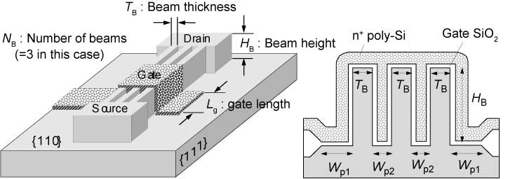
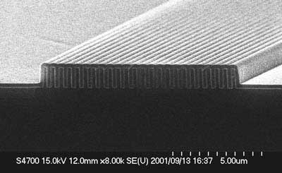
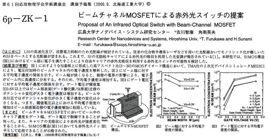
�@ �@���ꂪ�A1999�N�ɒ�Ă����u���R�d�q�i�t���[�L�����A�j�z���ɂ������W�����[�^�v�ł���A2006�N�ɏ��߂ē���ɐ��������B2007�N�ɂ͂���ɍ��������œ��삵���B���̃A�C�f�B�A�͉�X�����E�ɐ�삯�Ĕ��Ă����ƍl���Ă������A�_�����e�����ۂ̃��t���[����1991�N�ɓ����A�C�f�B�A�����ɘ_�����\����Ă������Ƃ�2008�N8���ɒm��iG. V. Treyz, Paul G. May, Jean-Marc Halbout, "Silicon Optical Modulators at 1.3 ��m Based on Free-Carrier Absorption," IEEE Electron Dev Lett., Vol. 12, No. 6, pp. 276-278, June 1991)�B�܂��A���ʂƂ��Č��ɂ͑f�l�����������ߋ���R&D������m�炸�ɍl���o�������Ƃ����炻�̊댯���͂��������A���炽�߂Č������莞�̒������d�v�ł��邱�Ƃ�������B���L��R&D�̌o�܂��q�ׂ�B �@���A�Ƃ��ɐԊO�����z�����鎩�R�d�q�i�t���[�L�����A�j�ɋ߂������̔��]�L�����A��p���邽�߁A���̔��]�L�����A��MOS�g�����W�X�^�̃Q�[�g�ő������邱�Ƃ��l�����B���Ƃ��Ǝ��R�d�q�ƐԊO���̑��ݍ�p�͋����Ȃ�����A�ɗ͔��]�L�����A�̖��x��傫�����邽�߁A�����^�̃g�����W�X�^�����삵���B���ꂪ�}�P�Ɏ����r�[���`���l���g�����W�X�^�ł���A���������\���̈ꕔ��}2�Ɏ������B
�@�����1�N����2000�N9���̏H�G���p�����w��ŁA�f�o�C�X����ƕ��s���čs���Ă����ԊO���z���V�~�����[�V�������ʂ\�����B�}3�ɂ��̗\�e�������B�Ȃ��A���W�����[�^�ƃX�C�b�`�͓��`��Ƃ��ėp���Ă���B
 (a) ���Ր}�@�@�@�@�@�@�@(b) �f�ʐ} �}1�@Si�r�[���`���l���g�����W�X�^ |
 �}2�@������Si�ŕ���ꂽ31�{��Si�r�[�� |
�}3 2000�N9���E�H�G���p�����w��ɔ��\�������X�C�b�`�̒��
�@���X�C�b�`�Ƃ��Ă̓���͐������Ȃ������B�����炭�B��ő�̌�����SOI(silicon-on-insulator) ���p���Ȃ��������Ƃł��낤�B�������莞��SOI�������ł��Ȃ��������Ƃ����ڂ̌����ł��邪�A���[�U�[���ƌ��H�̈ʒu�I���킹���x���Â��l���Ă������Ƃ������ł���B���˂����ԊO�����قƂ�ǂr������ɔ����Ă��܂��A������̃r�[�����ɗ��܂�Ȃ��������ʂł���B�����^�g�����W�X�^�����삷�鎞�Ԃ͂Ȃ��������ASOI���ɂ������߂��ē`�������Ԃ͐}4�Ɏ����悤�Ɋm���߂��B
�@�{���̖ړI�͐������Ȃ��������A�r�[���`���l���g�����W�X�^�Ƃ��Ă̓���͖����ł�����̂ł���A �O�����g�����W�X�^�̍��ŏq�ׂ����Ƃ��g�����W�X�^�Ƃ��Ă̓���\�����B���̌�������O�����g�����W�X�^�������n�܂����B
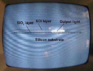 �}4�@SOI�w����`�����ďo�˂���1.55mm�ԊO���o�́i�ԊO�r�f�I�J�����o�́j |
| ���O�����\�� ���@T. Furukawa, H. Yamashita, and H. Sunami, �gCorrugated-Channel Transistor (CCT) for Area-Conscious Applications,�h Extended Abstracts of International Symp. on Solid State Devices and Materials, Abs. No. A-3-2, pp. 139-140, Nagoya, Sept. 17-19, 2002. ���@T. Furukawa, H. Yamashita,?and H. Sunami, �gA Proposal of Corrugated-Channel Transistor (CCT) with Vertically-Formed Channels for Area-Conscious Applications,�h Jpn. J. Appl. Phys., Vol. 42, Part 1, No. 4B, pp. 2067-2072, April 2003. |
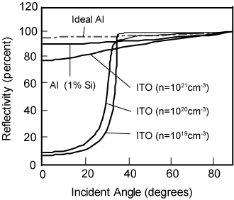
�@�����ŁA���d�������肩�����œ�����ITO(indium tin oxide)�̓K�p���l�������A���Ƃ���Si�ɔ�ׂ�Ή������ꂽITO�̂悤�ȁh�����g�ޗ����r���W�σv���Z�X�Ɏ������ނ͖̂��ł���̂ő��̍ޗ����l�����B�܂��AAl�͔��˗��������̂Ŗ]�܂����悤�ɍl�����邪�A���d�����������t���[�L�����A�������]�܂����Ȃ��B�������ʂ̈ꕔ��}5�Ɏ����B
 �}5�@�œK�N���b�h�ޗ��̑I�� |
 �}6�@���g�H���ȕ��̍œK�� |
 �}7�@SOI���g�H�����1.55mm�o�ˌ� |
�@�����ŁA�����Ƃ����䂵�₷���W�σv���Z�X�Ƃ̑����̂悢�������V���R�����N���b�h�Ƃ��đI�������B �R�A�Ƃ̊ԂɓK���Ȍ����̃V���R���_���������ނ��Ƃɂ���đ������V���R�����̃t���[�L�����A�̉e�������Ȃ�����\����ݒ肵���B
�@�܂��A���ˌ������ڏo�͌��ɉ����Ȃ��悤�ɓ��g�H��90�x�܂���̂ŁA�œK�Ȍ`���I�������B�}5�Ɏ������̂ł�No. 1���ł��D��Ă����B �������ʂ𑍍����� ���g�H��v���A�Ⴂ�z�����ŐԊO�����`�����邱�Ƃ��m�F�����B�}7�ɏo�ˌ��̗���������B�~�`�̃r�[�����A�Ȃ��Č����邪�A�����}���`���[�h�œ`�����Ă��邱�Ƃ�\���Ă���B
���@M. Kawai, K. Endo, T. Tabei, and H. Sunami, �gAn Experimental Analysis of 1.55-mm Infrared Light Propagation in Integrated SOI Structure,�h Extended Abstracts of International Symp. on Solid State Devices and Materials, Abs. No. P7-1, pp. 556-557, Tokyo, Sept. 15-17, 2004.
 �}8�@���삵�����g�H�ƌ��o�� |
 �}9�@���W�����[�V�������� |
 �}10�@���W�����[�V�����̃Q�[�g����d���ˑ��� |
���@Tomoki Hirata, Kenta Kajikawa, Tetsuo Tabei, and Hideo Sunami, �gProposal of a Silicon Optical Modulator Based on Inversion-Carrier Absorption,�h Extended Abstracts of International Symp. on Solid State Devices and Materials, pp. 280-281, Tokyo, Sept. 19-21, 2007.
���@Tomoki Hirata, Kenta Kajikawa, Tetsuo Tabei, and Hideo Sunami, �gProposal of a Metal-Oxide- Semiconductor Silicon Optical Modulator Based on Inversion-Carrier Absorption,�h Jpn. J. Appl. Phys., Vol. 47, No. 4, pp. 2906-2909, 2008.
 �}11�@���삵�����g�H�ƌ��o�� |
 �}12�@���W�����[�V�������� |
 �}13�@���W�����[�V�����̃Q�[�g����d���ˑ��� |
���@Kenta Kajikawa, Tetsuo Tabei, and Hideo Sunami, �gSilicon Optical Modulator Based on Accumulation-Carrier Absorption of Metal-Oxide-Semiconductor Capacitor Waveguide,�h Extended Abstracts of International Symp. on Solid State Devices and Materials, Abs. No. E-2-2, pp. 104-105, Tsukuba, Sept. 23-26, 2008.
���@Kenta Kajikawa, Tetsuo Tabei, and Hideo Sunami, �gAn infrared Silicon Optical Modulator of Metal-Oxide-Semiconductor Capacitor Based on Accumulation-Carrier Absorption,�h Jpn. J. Appl. Phys., Vol. 48, No. 4, pp. 04C107-1-4, 2009.
�@���̉�͂ł́A�d������������Ƃ��̌����x�̕ω��ׂ����̂ŁA�d������������Ƃ��A�}14�Ɏ��������]�w��(���f)���ܗ��ω����l�����邽�߁A�ȉ��̂悤�Ɍv�Z���s�����B
�@�܂��R�A/�N���b�h�\����Si/������Si�Ɗȗ������āAMarcatili�ߎ�(�Q�l�����Q�Ɓj��p���ē��g�H����`��������̔g���x�N�g�����Z�o�B
�A�g���x�N�g������R�A/�N���b�h���E�ʂւ̓��ˊp�ƒP�ʒ���������̔��ˉ��Z�o�B
�B�}14�Ɏ�����Ă���Si/���]�w/SiO2/������Si���w�\���ցA�A�ŎZ�o�����p�x�œ��˂������̔��˗��Ɣ��˂̉���`�������x�̕ω����Z�o�����B
 �}14�@��͂��s�����\�� |
 �}15�@���`���g�` �i���]�w�z���͊܂߂��N���b�h�ɂ��z���̂݁j�j |
 �}16�@�����Ƃ̔�r |
�@ �@��͂̌��ʁA�}15�Ɏ����悤�ȓ`���g�`���B�܂��A��L�̎������ʂƔ�ׂ����ʂ�}16�Ɏ������A��ʓI�ɂ��悭���v���Ă���Ƃ����悤�B�܂��A���̂悤�ȌX�������邱�Ƃ����������B
(1) �����̃��[�h�قǑ�����Si�ɂ�鑹�����傫���F���g�H���ł̔��ˉ͍����ɂȂ�قǑ����Ȃ�̂ŁA����[�h���x�z�I�ł���A�}15�̎������ʂ͂��̂��Ƃ��悭�����Ă���B
(2) �Q�[�g�_�����������قǏ����䂪�������Ȃ�F����̓Q�[�g�_�����������قnj����R�A�����ɕ����߂���ʂ������Ȃ�A���Ɣ��]�w�d�q�̑��ݍ�p���������Ȃ邽�߂ƍl������B�����ߌ��ʂ�����������ɂ̓Q�[�g�_�������ł��邾���������A�\�Ȃ���ܗ����R�A�ł���Si�ɋ߂��ق������ʓI�ł���B
���@Tetsuo Tabei, Tomoki Hirata, Kenta Kajikawa, and Hideo Sunami, �gPotentiality of Silicon Optical Modulator Based on Free-Carrier Absorption,�h Technical Digest of IEEE Internat. Electron Devices Meeting, pp. 1023-1026, Washington, D. C., Dec. 10-12, 2007.
���@Tetsuo Tabei, Tomoki Hirata, Kenta Kajikawa, and Hideo Sunami, �gPotentiality of Metal-Oxide-Semiconductor Silicon Optical Modulator Based on Free Carrier Absorption,�h Jpn. J. Appl. Phys., Vol. 48, No. 4, pp. 114501-1-7, 2009.
���@E. A. J. Marcatili, "Dielectric Rectangular Waveguide and Directional Coupler for Integrated Optics," Bell Syst. Tech. J., Vol. 48, pp. 2071-2102, 1969.
�@
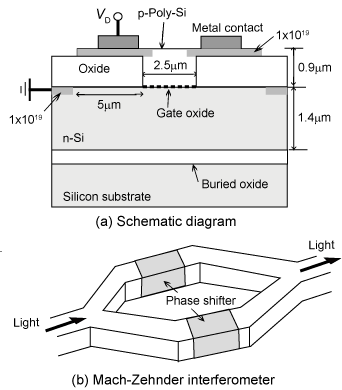 �}17�@�C���e�����\�̃��W�����[�^�\�� |
 �}18�@�}�b�n�c�F���_�[�^�Ǝ��R�d�q�z���^ |
�@�}�b�n�c�F���_�[�^�͂����킸���̌��H���̕ω���p����̂ŁA�}18(a)�Ɏ������Ƃ��g���ɑ���ˑ������ɂ߂đ傫���A�����I�ɂ������̔g���Ƃ��̋ߕӂ̋����g�������p���邱�Ƃ��ł��Ȃ��B����ɂ����X�̒�Ă��郂�W�����[�^�͊��v��p�����t���[�L�����A�̋z���ɂ��ω��𗘗p������̂ł���A�}18(b)�Ɏ������Ƃ����̔g���ɂ��ω����ɂ߂ď������B�܂葽���̈قȂ�g���̌����ɕϒ����邱�Ƃ��ł���_�ɓ���������A�V���ȉ��p�̉\�����������̂ƍl���Ă���B
���@Ansheng Liu, Richard Jones, Ling Liao, Dean Samara-Rubio, Doron Rubin, Oded Cohen, Remus Nicolaescu, and Mario Paniccia, "A high-speed silicon optical modulator based on a metal-oxide-semiconductor capacitor," Nature pp. 165-167, 2004.
Motivation of research �@Soon after I began with doing research at Research Center for Nanodevices and Systems, Hiroshima University in 1998, I made up my mind to contribute to the center as well as to realize 3-D device ideas which I had devised while working in a company. Since the center was known as one of proposers of optical integrated circuits I started a small project in silicon optoelectronics field.
�@A research target of this project was an optical modulkator based on free-carrier absorption. We succeeded in an operation of the mudulator first in 2006. Furthermore, much more efficient operation was obtained in 2007. We thought that this modulation mechanism had been proposed first by us at that time. But we realized in August 2008 that this idea had already been proposed by pioneers (G. V. Treyz, Paul G. May, Jean-Marc Halbout, "Silicon Optical Modulators at 1.3 mm Based on Free-Carrier Absorption," IEEE Electron Dev Lett., Vol. 12, No. 6, pp. 276-278, June 1991) when we got suggestions from a journal paper reviewer.
�@When I, as a nonprofessional engineer in the field of optoelectronics, proposed this idea, there existed some possibilities that this had already been proposed by others. This became real. We realized that an invenstigation for prior works was essential when we set about the new research. The procedure of the research is described here. �@
�@
PAbsorption analyses together with fabricated devices were presented at the fall meeting of Japan Society of Applied Physisc in September 2000, as shown in Fig. 3 one and half years after the research start.
 Fig. 1 Schematic diagram of silicon beam-channel transistor |

Fig. 2 31-silicon beams covered by polysilicon film |
Fig. 3 A proposal of an optical switch presented at the fall meeting of Japan Society of Applied physics.
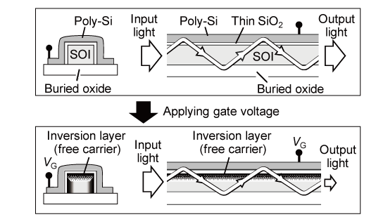
PWe did not succeeded in oprtical switching. Major reason was speculated that we did not use silicon-on-insulator, SOI substrate. We did not have that substrate at the research start and we thought alignment accuracy was not so critical for the light beam and the silicon beam as an optical waveguide. Therefore, input infrared light almost ran away from the waveguide going through the silicon substrate. We could not afford to fabricated another transistor with SOI substrate however, we confirmed that infrared light was confined inside SOI waveguide as shown in Fig. 4.
PWe could not achieve the original target plan however, we succeeded in beam-channel transistor operation as descived in 3-D transistor section. From this research results, 3-D device project started.
Fig. 4 1.55mm infrared output light come from SOI waveguide(infrared video camera image). |
<Publication>
�� T. Furukawa, H. Yamashita, and H. Sunami, �gCorrugated-Channel Transistor (CCT) for Area-Conscious Applications,�h Extended Abstracts of International Symp. on Solid State Devices and Materials, Abs. No. A-3-2, pp. 139-140, Nagoya, Sept. 17-19, 2002.
�� T. Furukawa, H. Yamashita,?and H. Sunami, �gA Proposal of Corrugated-Channel Transistor (CCT) with Vertically-Formed Channels for Area-Conscious Applications,�h Jpn. J. Appl. Phys., Vol. 42, Part 1, No. 4B, pp. 2067-2072, April 2003.
PTherefore, we have chosen first indium-tin oxide, ITO which was considerably conductive and transparent at visible light regime. But ITO is"dirty" as compared with highly purified silicon. Therefore it may make troubles in silicon integrated circuit fabrication. While, aluminum film which has high reflectivity was estimated to be suitable, but plenty of free carriers disturb light absorption by inversion carriers. A part of analyses is nshown in Fig. 5.
Fig. 5 Selection of suitable clad material. |
Fig. 6 Selection of suitable bend structure. |
Fig. 7 1.55-mm output light at waveguiide end. |
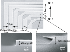
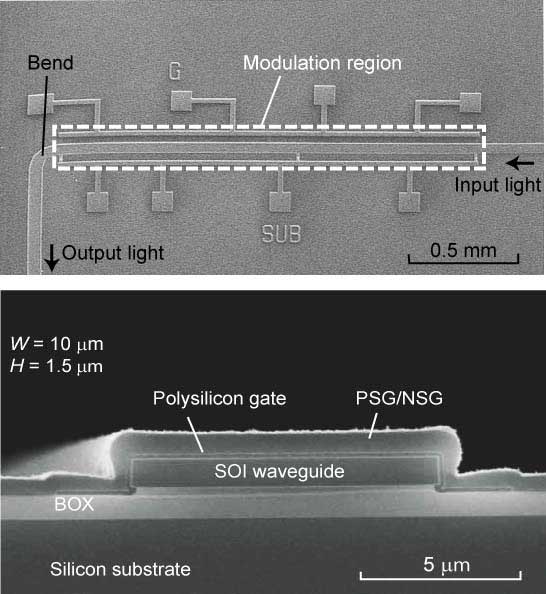
PThus, we have chosen polysilicon as the clad. It is easily deposited and has good compatibility with integrated circuit fabrication processes. By putting a silicon dioxide film with appropriate thickness in between clad and core, an influence of free carriers in the polysilicon clad was weakened.
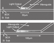
PIn addition, an optimum design for 90-degree bend structure was chosen to avoid input light coming into output light �@A structure of No. 1, as shown in Fig. 6, was confirmed to be most suitable. Taking total analyses into consideration, adequate waveguides were fabricated resulting in satisfactory results for light propagation with low loss. Figure 7 shows an example. This shows multi-mode propagation of the light.
�� M. Kawai, K. Endo, T. Tabei, and H. Sunami, �gAn Experimental Analysis of 1.55-mm Infrared Light Propagation in Integrated SOI Structure,�h Extended Abstracts of International Symp. on Solid State Devices and Materials, Abs. No. P7-1, pp. 556-557, Tokyo, Sept. 15-17, 2004.
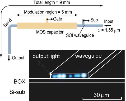
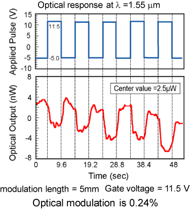
Fig. 8 Fabricated modulator and the output light. |
Fig. 9 A modulation result. |
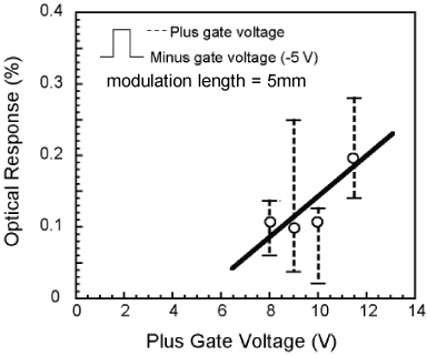
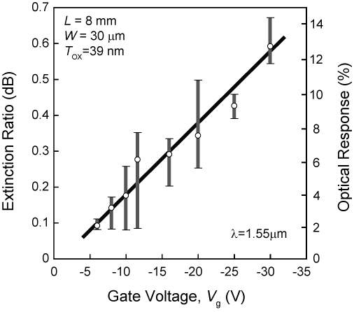
Fig. 10 Applied gate voltage dependence of optical response. |
�� Tomoki Hirata, Kenta Kajikawa, Tetsuo Tabei, and Hideo Sunami, �gProposal of a Silicon Optical Modulator Based on Inversion-Carrier Absorption,�h Extended Abstracts of International Symp. on Solid State Devices and Materials, pp. 280-281, Tokyo, Sept. 19-21, 2007.
�� Tomoki Hirata, Kenta Kajikawa, Tetsuo Tabei, and Hideo Sunami, �gProposal of a Metal-Oxide- Semiconductor Silicon Optical Modulator Based on Inversion-Carrier Absorption,�h Jpn. J. Appl. Phys., Vol. 47, No. 4, pp. 2906-2909, 2008.
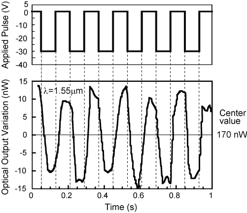
Fig. 11 Fabricaed waveguide and output light. |
Fig. 12 Modulationm result. |
Fig. 13 Gate voltage dependence of extinction ratio |
�� Kenta Kajikawa, Tetsuo Tabei, and Hideo Sunami, �gSilicon Optical Modulator Based on Accumulation-Carrier Absorption of Metal-Oxide-Semiconductor Capacitor Waveguide,�h Extended Abstracts of International Symp. on Solid State Devices and Materials, Abs. No. E-2-2, pp. 104-105, Tsukuba, Sept. 23-26, 2008.
�� Kenta Kajikawa, Tetsuo Tabei, and Hideo Sunami, �gAn infrared Silicon Optical Modulator of Metal-Oxide-Semiconductor Capacitor Based on Accumulation-Carrier Absorption,�h Jpn. J. Appl. Phys., Vol. 48, No. 4, pp. 04C107-1-4, 2009.
�@
PIn these analyses, light intensity variation under gate voltage application was aimed to be analyzed. To take into consideration complex refractive index, assumptions were made as follows;
(1) wave number vector was calculated with a simplified structure consisting of silicon core and polysilicon clad structure;
(2) number of reflecting times was calculated by incident angle of light and waveguide length from wave vector;
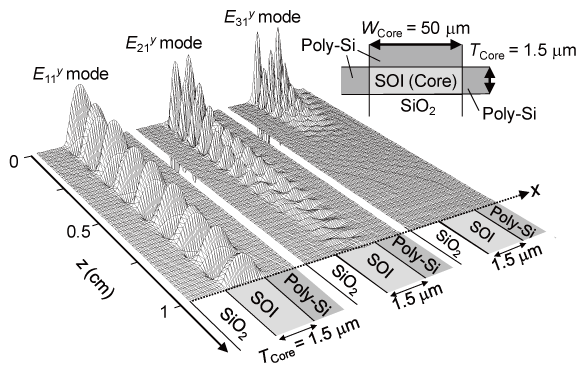
(3) propagation light intensity was calculated with number of reflecting times nad incident angle at silicon/ inversion layer/ SiO2/ polysilicon structure, as shown in Fig. 14.
Fig. 14 A structure analized. |
Fig. 15 Propagation wave forms without inversion carrier absorption. |
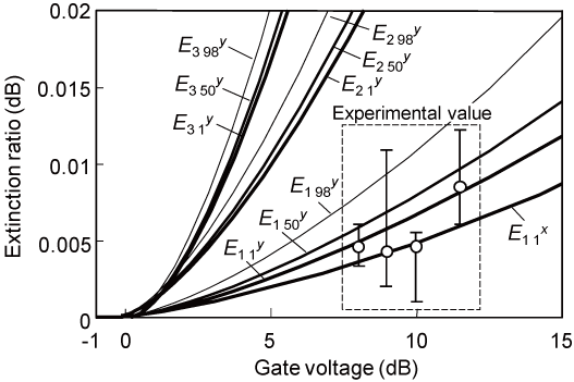
Fig. 16 Comparison with experimentals. |
PThe analyses generated light propagation characteristics. One exmple is shown in Fig. 15. In addition, comparison between analyses and experimentaal results is nshown in Fig. 16. They coincide well each other. In analyses, characteristics as descibed below were found.
(1) Loss with polysilicon is enhanced at highr mode : since number of reflection tiems increases with the increase in grade of mode, lower mode of propagation becomes dominant as shown in Fig. 15.
(2) Extinction ratio becomes smaller with the increase in gate oxide thickness : the thicker gate oxide enhances confinement of light inside core resulting in less interaction between the light and inversion carriers. To reduce the confinement effect, thinner gate oxide and the refractive index which is equivalent to that of core silicon are desirable.
�� Tetsuo Tabei, Tomoki Hirata, Kenta Kajikawa, and Hideo Sunami, �gPotentiality of Silicon Optical Modulator Based on Free-Carrier Absorption,�h Technical Digest of IEEE Internat. Electron Devices Meeting, pp. 1023-1026, Washington, D. C., Dec. 10-12, 2007.
�� Tetsuo Tabei, Tomoki Hirata, Kenta Kajikawa, and Hideo Sunami, �gPotentiality of Metal-Oxide-Semiconductor Silicon Optical Modulator Based on Free Carrier Absorption,�h Jpn. J. Appl. Phys., Vol. 48, No. 4, pp. 114501-1-7, 2009.
�� E. A. J. Marcatili, "Dielectric Rectangular Waveguide and Directional Coupler for Integrated Optics," Bell Syst. Tech. J., Vol. 48, pp. 2071-2102, 1969.
Fig. 17 A modulator structure Intel published. |
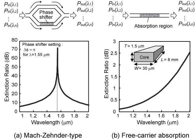
Fig. 18 Mach-Zehnder type (a) and free-carrier absorption type (b). |
PSince Mach-Zehnder type interferometer uutilizes very small variation of optical length, extinction ratio strongly depends on wavelength of the light as shown in Fig. 18 (a). Therefore, bandwidth of the light is very narrow. Otherwise, free-carrier absorption type which we have proposed depends very weakly on wavelength as shown in Fig. 18 (b). Thus, this features simultaneous modulation for wide range of propagation light leading to some novel application.
�� Ansheng Liu, Richard Jones, Ling Liao, Dean Samara-Rubio, Doron Rubin, Oded Cohen, Remus Nicolaescu, and Mario Paniccia, "A high-speed silicon optical modulator based on a metal-oxide-semiconductor capacitor," Nature, pp. 165-167, 2004.
All Rights Reserved, Copyright (C) 2009 Hideo Sunami